Intel bets on outmuscling Arm in the RAN
The US chipmaker reckons the RAN industry is too small to keep pace with design changes that will benefit its general-purpose processors, but not everyone is convinced.

Perform surgery on Nokia's latest radio equipment and you would quickly stumble across transistors based on relatively new 5-nanometer process nodes. They were probably made at a foundry in Taiwan, the island source of most advanced components. Go back three years and you would not have encountered them in the telecom sector outside the most expensive smartphones. Their introduction into radio access network (RAN) equipment shows how fast kit makers have moved to exploit state-of-the-art silicon.
When it comes to process nodes, the smaller the measurement, the better the chip. Shrinkage, very crudely, allows a chipmaker to cram more transistors onto the same bit of silicon. For a company like Nokia, this means higher-performance products that guzzle less power. Tommi Uitto, the head of the Finnish vendor's mobile networks business group, ticks off all the different areas to benefit – capacity, connectivity, energy consumption and product cost.
But there is doubt this market for customized RAN silicon – so-called application-specific integrated circuits (ASICs) – will be able to adapt so quickly in future. Each year, the broader RAN market generates between $40 billion and $45 billion in sales, depending on which analyst firm you ask. The overall market for semiconductors, meanwhile, hauled in about $574 billion last year, according to the Semiconductor Industry Association (SIA). At its dwarfish size, the RAN market simply lacks the research and development (R&D) muscle to keep jumping quickly from one process node to the next.
Figure 1:  Construction equipment preparing the site for two Intel factories in Arizona.
(Source: Intel)
The limits of performance
Such is the claim of Intel, which spies an opportunity to divert billions of dollars in future RAN spending away from custom silicon products and into its x86, "general purpose" processors. "We keep delivering and refreshing every 18 to 24 months," said Sachin Katti, the head of Intel's network and edge group, during an interview with Light Reading at this year's Mobile World Congress. "Custom silicon cannot afford to refresh its design every 18 to 24 months because the market is much smaller."
The logic is compelling. Intel reported total revenues of $63.1 billion last year, making it substantially bigger than the entire RAN industry. At its data center and AI group, which mainly supplies x86 chips for server central processing units (CPUs), sales were about $19.2 billion. The same underlying technology is used across these chips and those Intel is pitching for the RAN – hence the general-purpose label. This gives Intel a much larger addressable market and a bigger pot of money to reinvest.
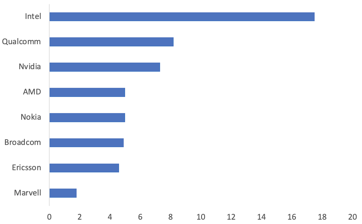
Figure 2: R&D spending for most recent fiscal year ($B)  (Source: companies)
The cry has been taken up by Intel's partners and telcos impressed by the rhetoric. They include Rakuten, which has used Intel chips to build a fourth mobile network in Japan and designed software it markets to other telcos on top of Intel's silicon. "Because of the volume used, there is a massive amount of R&D invested behind it to provide the next and the next and the next generation," said Rabih Dabboussi, the chief business officer of Rakuten Symphony, Rakuten's vendor subsidiary. "That is why we've seen these CPUs pushing the limits of performance of an ASIC developed by a specific vendor."
Ericsson, one of the world's biggest developers of RAN silicon, concedes that general-purpose processors have been able to narrow the gap with its ASICs. Last year, it spent about $4.6 billion on R&D, and not all of that will have gone toward those ASICs, with cloud RAN identified as another focus area in recent earnings reports. Nokia spent about $5 billion, spread across various network and software divisions. Intel's own R&D budget topped $17.5 billion.
Arm wrestling
But this battle for the RAN is not a straightforward contest between Intel on one side and a couple of network equipment makers on the other. Nor is it simply about process nodes. The ASICs found in most traditional RAN infrastructure use blueprints drawn up by Arm, a UK-based company today owned by Japan's SoftBank. Just as Intel is omnipresent in servers, so Arm is best known as the architecture that underpins most of the world's smartphones. Yet each has made incursions into the other's territory.
There are important differences between them. At the technical level, x86 is a complex instruction set computing (CISC) architecture, whereas Arm uses reduced instruction set computing (RISC). While the many details are beyond the scope of this article, and the distinctions are blurring, RISC is generally seen as a more lightweight and power-efficient option.
The best everyday example is the Arm-based M1 processor developed by Apple for its latest computers. Anyone who has replaced an older, Intel-based MacBook with an M1 model will not have missed the sound of the internal fan whirring like helicopter blades before take-off. And Apple does not seem to have given up anything in speed or features. Quite the opposite, in fact.
Figure 3:  An Apple R&D facility in Munich, Germany, where silicon is designed.
(Source: Apple)
The big difference commercially is that Arm, unlike Intel, does not make chips. Instead, it licenses its designs to numerous manufacturers, Apple among them. On the RAN side, it has previously counted big equipment makers such as China's Huawei as customers. But its licensees also include semiconductor specialists like Broadcom, Marvell, Nvidia and Qualcomm. Contributing their own technical wizardry on top of Arm's blueprints, these companies have traditionally worked with Ericsson and Nokia on the ASICs for the Nordic vendors' own equipment.
Arm's advocates say x86 is suboptimal for the compute-intensive baseband processing that takes place within the RAN (what's referred to as the Layer 1 part of the RAN software stack). And there is some anecdotal evidence from operators. Andrea Dona, the chief network officer of Vodafone UK, noted an increase in energy consumption when his company tried running baseband functions on x86 processors, he told Light Reading during a meet-up with analysts and reporters in London this week.
Even AMD, the other big vendor of x86 processors, endorses Arm in this area. "What Arm is great at is high-level acceleration, high performance of the Layer 1 components," said Nick Hancock, the director of the telco vertical at AMD. "In terms of flexibility of writing code and ease of portability and the rest of it, x86 is the right answer for Layers 2 and 3. That's the conclusion most of the industry has so far come to. I don't see that fundamentally changing."
Virtualization commotion
Why, then, would anyone consider x86 in the first place? The short answer is that it remains the simplest approach for telcos trying to virtualize the RAN. In traditional ASICs, there is a tight bond between hardware and software that effectively makes them a vertical silo. Break them apart and a telco could host its RAN software on the same hardware and cloud platforms used to support other network functions and IT workloads.
This virtualization essentially means using general purpose processors, and that market is currently dominated by Intel and AMD. Indeed, according to recent data from Counterpoint Research, Intel served about 71% of the market for data-center CPUs last year, while AMD's share was almost 20%, leaving only a 9% slice to others, including Arm licensees.
As AMD's Hancock points out, nobody in the telco sector ever disputes the suitability of x86 for Layers 2 and 3 in the RAN software stack. Introducing custom silicon for Layer 1 via a technique dubbed inline acceleration risks adding complexity and cost. It would also be a barrier to virtualization, claims Intel's Katti.
Those ASICs would not be a shared resource and an operator would not be able to upgrade software with the same Kubernetes tools used everywhere else, he previously told Light Reading (Kubernetes is the main open-source platform for managing cloud-native software). The operator, moreover, would be "locked into" one vendor's hardware and software package, he said.
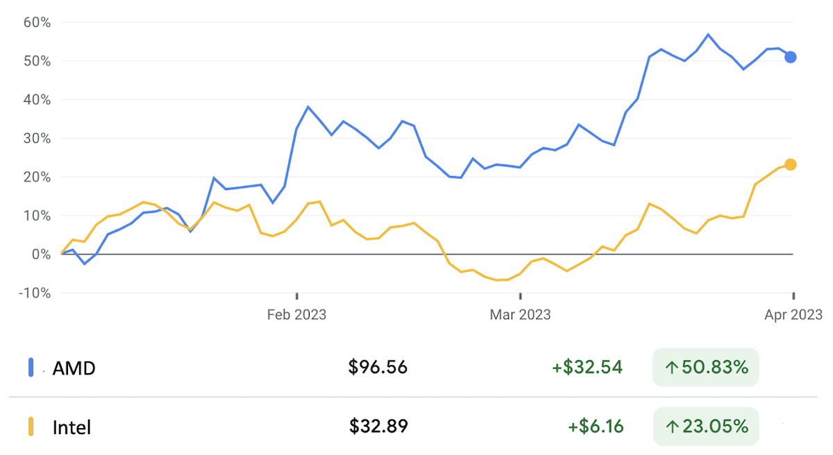
Figure 4: AMD and Intel on the Nasdaq this year  (Source: Google Finance)
But some of these points are now disputed. For a start, Intel's own Layer 1 offer includes a reference design called FlexRAN that looks equally bad when it comes to lock-in. While no one is forced to use it, software written on top of FlexRAN cannot be ported to other silicon platforms, according to Yago Tenorio, Vodafone's network architecture director. And those include x86 chips from AMD. "The way the license is written is that it can only be used on Intel processors," said Hancock. "It is like having a car but not the keys."
Numerous sources have also told Light Reading that companies such as Red Hat, VMware and Wind River do allow the same Kubernetes tools to be used across this kind of estate. Some of the Internet giants seem to offer that capability, as well. "You need to have a VMware or a Red Hat or an AWS hardware abstraction layer that will make the software independent of the hardware," said Gilles Garcia, a senior business director at AMD.
And what of sharing? One benefit of virtualization is being able to pool hardware resources and allow unrelated functions to use them. A data center home to central units, which process Layer 2 and 3 software, could theoretically support other workloads. But there is little expectation the distributed units responsible for Layer 1 are going to reside anywhere except at the base of towers, where other workloads will probably not be relevant. If network topology reserves custom silicon for Layer 1, worrying it cannot be used for anything else seems pointless.
Merchant shipping
The caveat is the cost of this additional silicon, usually stored on network interface cards (NICs or SmartNICs) that can be slotted into servers. That debate is already raging in the core network domain, said AMD's Hancock. "If you look at the major players in core today, there is no doubt they are considering if the economics of having SmartNICs to do offloading makes sense."
Nevertheless, the emergence of Marvell, Qualcomm, Nvidia and potentially others as developers of "merchant silicon" for Layer 1 is arguably the biggest recent change in the RAN market, and the greatest threat to Intel's RAN ambitions. For the most recent fiscal year, those three companies had combined R&D spending of more than $17.3 billion, roughly the same amount Intel invested over this period. And there is little sign they are falling behind on process nodes.
All three are already buying 5-nanometer chips from Taiwanese foundry TSMC, while Intel is struggling to mass produce a 7-nanometer chip, according to one high-level industry source who spoke with Light Reading on the condition of anonymity. Sapphire Rapids, the name for Intel's latest generation of Xeon-branded processors, was delayed multiple times before it finally landed this year. Intel's depressed share price, which has halved in the last two years, reflects investor concern about its roadmap and efforts to become a foundry.
Intel will need to avoid future delays if it is to restore confidence. Under its ambitious plans, its next generation of processors is supposed to use 3-nanometer technology. Yet there is skepticism in the telecom sector that Intel will deliver. Success there would not guarantee an upset for Arm's licensees, but it would make the chest-thumping easier to sustain.
Related posts:
— Iain Morris, International Editor, Light Reading
About the Author(s)
You May Also Like


_International_Software_Products.jpeg?width=300&auto=webp&quality=80&disable=upscale)


