A Peek Into Infinera's PICs
The analyst ventures into Infinera's cleanroom for a closer look at photonic integrated circuit production

Recently, I toured Infinera Corp. (Nasdaq: INFN)'s photonic integrated circuit (PIC) manufacturing facility in Sunnyvale. I'm told I was the first member of the media to tour the closely guarded fab, and for me, it was my first-ever IC fab experience. This column is a sneak peek into the manufacturing facility that now produces about 40 percent of North America's long-haul DWDM capacity – a remarkable statistic, given that six years ago this fab was just starting production.
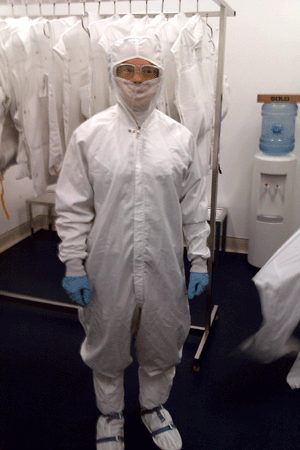
The first step of the tour is to suit up – head to toe in a white clean-room suit, the aim of which is to prevent the tiny particles of dust that people shed from landing on the tiny circuits in production and corrupting them.
The PICs are built in a clean-room facility. Clean rooms are classified according to the numbers of particles permitted in the air by volume. At the Infinera fab, rooms range from Class 1,000 (1,000 particles of equal to or greater than 0.5 micrometers per cubic foot) to Class 10 (just 10 particles equal to or greater than 0.5 micrometers per cubic foot). To put this in perspective: Urban air, according to Wikipedia, contains 35 million such particles per cubic foot. Even the paper on which I wrote these notes was a specialized paper designed to not shed particles.
The Infinera manufacturing process starts with indium phosphide (InP) wafers that Infinera purchases externally. The wafer material is one of the major differences between the Infinera PIC fab and an electronic IC fab. Silicon is good for many things, but not for emitting light; to build an efficient laser, indium phosphide is used. The Infinera wafers are circular sheets on which the Infinera PICs will be built. The size is important, because the bigger the surface area, the more PICs per wafer, which translates to greater volume and lower costs. All of the processing on those wafers, as well as the extensive testing, is done in Sunnyvale.
First, specialized semiconductor crystal growth reactors are used to deposit materials via chemical vapor deposition on top of the InP wafers – some of which, when grown, are just 10 to 20 atomic layers in thickness. The epitaxy process is repeated until all of the required materials are grown onto the wafers. The lithography steps take place in another room, the cleanest of all the clean rooms (a Class 10 room). As part of this process, a coating of photoresist material is uniformly spun onto the wafers. The process here is highly automated, using robotic systems to move the wafers from step to step. In fact, much of the Infinera manufacturing process is highly automated – a sharp contrast to the optical components manufacturing tours I participated in earlier in the decade. On those tours, I was amazed by how such state-of-the-art photonics were produced in such a manual, low-tech fashion; not so in Sunnyvale.
After photolithography, the InP wafers move to etching, where layers of substrate are moved from the portions of the chips that are not covered with the photoresist materials. Semiconductor etching has two components, a liquid "wet" process and a plasma "dry" process, and both etching processes are used on Infinera's wafers. In the wet etching bay, acids and solvents are used to remove the semiconductor materials from the unprotected areas on the chips.
The next step on our tour is metrology bay, where chip specs are tested using extremely powerful characterization tools, including x-ray diffraction tools, electron microscopes, and atomic force microscopes. Such tools are used to accurately measure features that are just tens to hundreds of angstroms in size. (An angstrom, or one ten-billionth of a meter, is the unit used for measuring atoms.)
By the time the die are cut from the wafers, they've already gone through a significant amount of testing – a key factor in Infinera's ability to produce high yields. The company will not disclose its specific yields but did share with me an interesting chart that showed its PIC outputs rising by 55 times during its first four years of production, while its number of wafer starts during the period remained relatively flat. Infinera said that part of the increase in PIC outputs during this period can be attributed to increased PICs per wafer, but that the vast majority of the output increase came from yield improvements. Based on the vendor's port-shipment reports, Infinera shipped about 8,400 PICs in 2009 (or 4,200 PIC pairs, including the transmit PIC and the receive PIC) – still very small volume when compared to electronic IC shipments.
One of the most interesting parts of the tour was the assembly process, through which the PICs are attached to submount, an off-the-shelf carrier that measures less than one-inch square. During the full assembly procedure, some three meters of gold wiring, thinner than a human hair, is spooled out to connect the many elements on the PIC to the carrier and package with such precision that none of those gold wires ever touch each other.
By the time the PICs leave Sunnyvale, they've been tested at the wafer level and the carrier (submount) level. They are then shipped to Infinera's Allentown, Pa., facility to be built into modules (the Infinera DTN DLM cards), and are tested again. In addition to the improved yields, a key benefit is a chip that doesn't fail in the field. The vendor attaches unique identifiers on every PIC and carrier chip that ships to help track down failures, but it has never put the system to use. Infinera reports that there has not been a single PIC failure in the field since inception, and counts more than 300 million field hours of continuous operation without a failure.
— Sterling Perrin, Senior Analyst, Heavy Reading
Read more about:
OmdiaAbout the Author(s)
You May Also Like


