Everyone needs to calm down about Huawei's Mate
Parts of the technology sector have taken Huawei's latest smartphone as proof of Chinese self-sufficiency in chips. It is nothing of the sort.

If Huawei had to cast itself in a cliched action movie, it would probably be as the embattled hero who finally overcomes adversity. In this script, its plane was shot down by US forces and it spent several years living off jungle rations, learning survival skills that have made it stronger and more independent than ever before. The Mate 60 Pro, the smartphone it released to much international fanfare this week, is supposedly the symbol of this never-say-die spirit and a big Chinese screw-you sign to the US.
The Shenzhen-headquartered equipment maker has spent a few years in the technological wilderness thanks to US sanctions cutting it off from vital components it needs for smartphones and network equipment. Perhaps worst of all was losing access to TSMC, a Taiwanese foundry that uses a mixture of Dutch and US equipment to produce the most advanced chips on the planet. At the bleeding edge, the transistors that feature in these chips measure just 5 nanometers, or billionths of a meter, and even smaller components are being developed.
Today, only Samsung can rival it, and the South Korean electronics giant is similarly reliant on Dutch and US tools. Sanctions forbid the sale of chips to Huawei if they were produced with any US expertise, cutting the Chinese company off from both TSMC and Samsung. Meanwhile, the Dutch government has been denying export licenses to ASML, whose ultra-violet lithography machines are a critical part of the chipmaking process. While ASML can still serve TSMC and Samsung (Taiwan and South Korea are its biggest markets), it is forbidden from selling its best equipment to Chinese foundries such as SMIC.
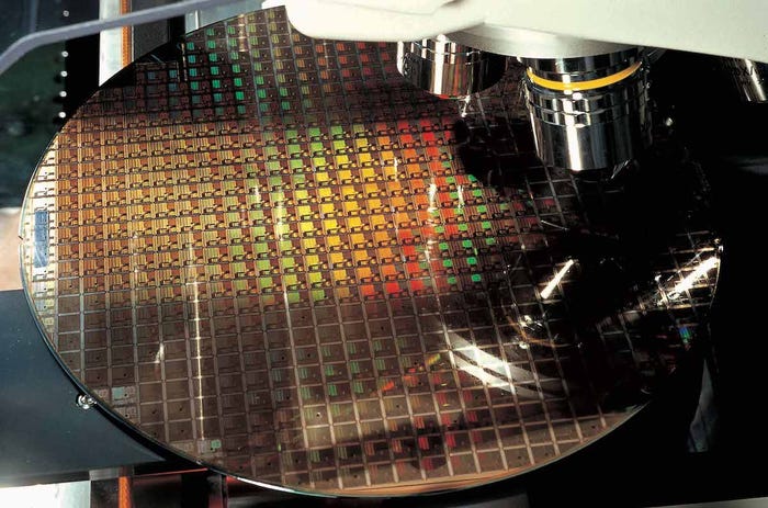
Figure 1:

A silicon wafer being processed inside one of TSMC's fabs.
(Source: TSMC)
But this did not stop SMIC from showcasing a 7-nanometer chip more than a year ago. ASML conceded at the time that a foundry could manufacture chips with these measurements without its state-of-the-art extreme ultra-violet (EUV) lithography machines. A slightly older process, known as deep ultra-violet lithography (DUV), would do, and ASML had been allowed to sell DUV machines to SMIC until a recent tightening of rules. The caveat is that DUV is not ideal. Producing lots of 7-nanometer chips at low cost would be difficult if not impossible.
SMIC's revelation last year did not stop many analysts and reporters from being apparently stunned when dissections of the Mate 60 Pro this week showed that 7-nanometer chips were a part of its inner circuitry. The "finding" was widely interpreted as evidence of Huawei's recovery and Chinese self-sufficiency in semiconductor technology. It is nothing of the sort.
'They are going backward'
For one thing, the inclusion of 7-nanometer chips would still leave Huawei at least one generation behind the latest iPhones and Samsung gadgets. Inevitably, performance would not be as good. For a company with a tarnished brand that has always based its marketing on technological proficiency, this will matter.
On the networking side, where decisions these days are largely about energy efficiency and a jumble of confusing technical specs, it will matter even more. Nokia's latest 5G basestation equipment includes 5-nanometer chips, and Tommi Uitto, the head of the Finnish company's mobile networks business group, has highlighted the advantages this would give Nokia over a so-called "high-risk vendor," the European designation for Chinese suppliers, stuck with older chips.
"When we are moving from 7 to 5 and then to 3, they are going backward," he told Light Reading at Mobile World Congress this year. "Comparing lesser to advanced silicon, you will take a hit in the radio unit power consumption. Power generates heat and that means a bigger and heavier product. You will also take a hit on the baseband side in capacity and connectivity and power consumption and product cost."
Consumers might not care as much, especially if they are Chinese and encouraged to buy local. The trouble is that one Mate 60 Pro dissected by Bloomberg and others is not proof Huawei can manufacture at scale. Denied access to ASML's EUV lithography machines, SMIC would struggle economically to produce components in large volumes, according to Richard Windsor, an analyst with Radio Free Mobile.
EUV monopoly
One of the reasons for Intel's loss of form in recent years was its attempt to use DUV technology to produce cutting-edge chips, he said. "Using a technique called double patterning, it is possible to manufacture a 7-nanometer chip (or even a 5-nanometer chip) using DUV equipment but, as Intel found out to its great cost, it doesn't work very well," Windsor wrote in a blog this week. "This means while one will get a few chips that work, a lot of the others will not, meaning that the cost to make one working chip will be far higher than is economical."
All this might need reappraising if Huawei begins shipping its Mate 60 Pro in vast quantities to considerable success. But ASML currently enjoys a monopoly in EUV lithography, and it spent a long time on developing that expertise. Most experts doubt China will be able to acquire a domestic EUV capability for many years. And by then, ASML may well have moved on to something even more advanced.
Huawei's gadget business took a massive hit because of US sanctions, with sales halving to just 243 billion Chinese yuan ($33 billion, at today's exchange rate) in 2021. Last year, they fell 12%, to RMB214 billion ($29 billion). And profitability has collapsed. Huawei's operating margin shrank to just 6.6% in 2022 from 19.1% the year before. The Mate 60 Pro has a lot of work to do.
Related posts:
— Iain Morris, International Editor, Light Reading
About the Author(s)
You May Also Like


_International_Software_Products.jpeg?width=300&auto=webp&quality=80&disable=upscale)


