Infineon Produces Chip Sandwich
Infineon claims to have produced the first multilayer electronic integrated circuit -- a chip 'sandwich,' if you will
August 12, 2002

Today, Infineon Technologies AG (NYSE/Frankfurt: IFX) announced what it claims is a breakthrough in chip packaging technology: a technique that allows two electronic ICs (integrated circuits) to be squeezed into the space formerly occupied by one (see Infineon Intros 'Sandwich' Chip System).
Put simply, the German chipmaker has come up with a way to solder two chips together, one above the other, using a layer of copper in which chip-to-chip interconnections can be formed.
Infineon claims that its technology offers "a way out of the wiring crisis" -- referring to the fact that the number of pin-outs on a chip, and the number of traces on a printed circuit board, are starting to limit the functionality that can be put inside the chip itself. Reducing those wires to short copper links inside a "sandwich" allows chips to run faster, take up less space, and could reduce costs by up to 30 percent, the company contends. Clever though it is, the idea of using stacked chips is not unique to Infineon. Others, including Sharp Foundry Services (part of Japanese electronics giant Sharp Ltd.) and Intel Corp. (Nasdaq: INTC), have developed so-called chip scale packages (CSPs) with up to four chips stacked on top of each other.
The different lies in the interconnects, says Reiner Schönrock, spokesperson at Infineon's worldwide headquarters in Munich. Stacked CSPs from other companies make connections using standard wire-bonding around the edges of the silicon die, rather than the copper sandwich developed by Infineon. "This [copper sandwich] is true 3D integration," Schönrock claims.
All stacked CSPs save on space and the costs associated with packaging, an approach that has turned out to be a big hit with manufacturers of mobile handsets. But Infineon's approach has several additional advantages over technologies from the likes of Sharp and Intel, which will open up other applications, says Schönrock.
For starters, the connections between chips are much shorter, so they can support faster speeds. The company claims that clock speeds of up to 200 GHz should be possible with its chips -- roughly 100 times faster than the fastest microprocessor today. This figure is a little hard to believe, but clearly this process has implications for fast communications technologies, including mobile and broadband networking.
The other key advantage is in heat dissipation. Since 80 percent of the chip's surface is covered by copper, which is a good conductor, the chip maintains an even temperature and can dissipate excess heat more easily. Furthermore, since the chip-to-chip interconnects are so short, they generate less heat in the first place than their wirebond counterparts.
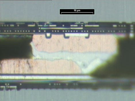
The above image, taken with a microscope, shows how the chips are melded together. Infineon uses a diffusion soldering process, called SOLID, for "solid liquid interdiffusion."
First, a layer of copper is applied to the two surfaces to be bonded. Patterns are created in the copper using standard photolithography techniques to define where the interconnections will go. Then a thin layer (3 microns) of solder is applied, and the surfaces are pressed together at 3 bar of pressure and 270 degrees C, creating a permanent bond. The backsides of the two silicon wafers have been pre-polished, so that when they are bonded together, their combined thickness is almost the same as an original single slice of silicon.
In the image, places where current is flowing appear bright. Copper, which shows up pink, forms a channel from the top chip to the bottom chip. The grey areas at the top and bottom of the image are cross-sections of plain silicon -- the electronics are only found in the surface layer of the wafer.
Infineon's first prototype 3D IC, produced for an unnamed smart-card vendor, integrates a memory chip with the smart-card controller, increasing the available memory from the usual maximum of 32 kbytes to 160 kbytes.
Proving that it works is the first step, says Schönrock, and now the company will look at partnering with other chipmakers to produce products that meet their needs. There is also an obvious opportunity to apply this technique to products that Infineon makes itself, such as VDSL gear. The company also "hasn't ruled out the possibility" of licensing its technology to other foundries, he adds.
— Pauline Rigby, Senior Editor, Light Reading
http://www.lightreading.comWant to know more? The big cheeses of the optical networking industry will be discussing this very topic at Opticon 2002, Light Reading’s annual conference, being held in San Jose, California, August 19-22. Check it out at Opticon 2002.
Register now and save $500 off the registration fee. Just use the VIP Code C2PT1LHT on your registration form, and deduct $500 from the published conference fee. It's that simple!
You May Also Like


_International_Software_Products.jpeg?width=300&auto=webp&quality=80&disable=upscale)


