Infinera CEO David Heard talks chips (and sciences)
Infinera CEO David Heard said that the US is doing the right thing by committing billions of dollars to semiconductor research and manufacturing. Since chips are such a big part of the price of the end product and the speed of product innovation, Heard said the recently passed CHIPS and Sciences Act could be a watershed moment in optical networking.

Infinera CEO David Heard is optimistic about what the CHIPS and Sciences Act can do for optical networking vendors, especially those that are endeavoring to be less dependent on foreign suppliers.
On Tuesday, August 9, President Joe Biden signed the bill that will provide $52.7 billion in subsidies for US semiconductor production and research, an attempt to make the US more competitive with China.
"The CHIPS and Science Act will boost American semiconductor research, development, and production, ensuring U.S. leadership in the technology that forms the foundation of everything from automobiles to household appliances to defense systems," said the White House, in a media statement posted last week.
Building semiconductors for the optical networking and telecommunications markets is a very capital-intensive business, Heard said. Since semiconductors are such a big part of the price of the end product and the speed of product innovation, it's critical to keep investing in R&D to drive better network performance.
"Today, almost 50% of the semiconductor revenues are from the US, and only 13% of the production comes from the US," Heard said.
He added that the government's investment could, if spent wisely, help companies continue a Moore's Law-like trajectory and "double the speed of innovation that we're able to bring to market."
You can download an unedited transcript of the podcast here.
Here are just a few things covered in this podcast episode:
What the CHIPS and Sciences Act does for companies like Infinera (01:38)
How it benefits the optical networking industry overall (06:33)
Infinera's reorganization and market acceptance (09:47)
The road to 800Gbit/s and the upcoming growth cycle. (13:39)
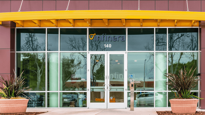
Figure 1:  Infinera headquarters in Sunnyvale, California, photographed in 2020.
(Source: Sundry Photography/Alamy Stock Photo)
Related stories and links:
Qualcomm, GlobalFoundries to expand agreement (press release)
Light Reading Podcast news, analysis and opinion
— Phil Harvey, Editor-in-Chief, Light Reading
About the Author(s)
You May Also Like


_International_Software_Products.jpeg?width=300&auto=webp&quality=80&disable=upscale)


