A cool components startup has popped up in Singapore with 3 shipping products, 100 staff, and its own fab plant
January 10, 2002

Singapore's DenseLight Semiconductors Pte Ltd. sprang a couple of surprises on the optical component community this morning when it came out of stealth mode with a funding announcement (see Integrated Optics Startup Gets $30M).
The first surprise is that DenseLight is already pretty well established. It's got six products, three of which are already shipping. It's also got 100 on staff and its own fully-operational, vertically-integrated fabrication facility.
All of this has been achieved since May 2000, when DenseLight was founded by a group of professors from Singapore's Nanyang Technological University (NTU).
The second surprise is that DenseLight appears to be having some success integrating active and passive devices in single indium phosphide chips -- a task that other startups have struggled with (see, for instance, Nanovation Comes Down to Earth).
That might explain why 3i Group PLC, a U.K. venture capital company, is betting big on DenseLight. It provided its $1.2 million seed funding and then stumped up a further $30 million in February 2001 so that it could remain the sole investor in the company.
"It was quite a gung-ho move on our part," admits Kain-Woon Yap, from 3i's Asia Pacific office, even allowing for the fact that 3i awarded the money in stages as it observed the startup's progress. He adds that the company will be more open to external funding going forward.
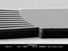
DenseLight is planning to make its chips using a process called "quantum-well intermixing." This enables it to grow a wafer and then modify the electrical and optical properties of selected parts of it using a diffusion process, to create multiple optical devices on the same chip.
It's worth pointing out that this is the same process used by another integrated-optics startup, Intense Photonics, Ltd., which, coincidentally, is also funded by 3i (see Intensive Care and Intense Photonics Puts on a Show).
Quantum-well intermixing is particularly useful for creating both active and passive devices on the same chip, says DenseLight's CTO Yee-Loy Lam. Passive devices need to be as optically transparent as possible, while active devices need to be absorptive.
The alternative to this is "regrowth" -- making a single device, then etching away a pit next to it, and growing new material in the hole. This works, but not very well, in Lam's view, because yields get progressively smaller with each regrowth step. "The beauty of quantum-well intermixing is that you make all the different bandgaps in a single go, so you don't suffer any yield loss," he claims.
By "bandgap," Lam is referring to a material's property that determines at which wavelength it emits light or absorbs it -- below the emission wavelength the material is transparent, above it, it is opaque.
There is more than one version of quantum-well intermixing, says Lam. DenseLight uses so-called "ion-implantation-based disordering," which involves shooting ions into the wafer in the places where the material's properties need to be changed. The ions disrupt the crystal lattice of the semiconductor, thus promoting diffusion inside the wafer when it is heated, he explains. When the material cools down again afterwards, the semiconductor recrystallises to become "as good as ever."
That said, a couple of DenseLight's products -- 2.5 Gbit/s direct-modulated distributed feedback (DFB) lasers and optical gain chips -- don't actually use quantum-well intermixing. It picked these as products because they address high-volume applications, according to Lam.
A third product which, like the two above, is available now, is a superluminescent light emitting diode (SLD). This type of device emits a broad range of wavelengths at high intensity, without actually lasing. It is used in high-performance sensors and some telecom headgear.
Denselight's SLDs use quantum-well intermixing to create a gradual 100 nanometer change in the output wavelength of the material across a 2-micron-wide stripe. As a result, the company obtains much higher power across all wavelengths than do its competitors, such as Opto Speed SA.
Lam says that DenseLight will release its first truly integrated products at the OFC show in March -- a tunable laser and an optical channel monitor. The tunable laser will be a simple three-section DBR laser with a 15nm tuning range, which is tuned by heating and cooling. Although plenty of vendors, including Agility Communications Inc., are developing lasers with faster and wider tuning, Lam believes there will be plenty of volume in narrowband devices, especially if they are produced cheaply enough. He sees quantum-well intermixing as the key to that.
The optical channel monitor will arguably be the company's most advanced product. "It will be the only channel monitor to monolithically integrate photodetectors with a passive component [an AWG]... providing that nobody else announces one before OFC," Lam claims. Making Arrayed Waveguide Gratings (AWGs) out of indium phosphide is a bit unusual. Bookham Technology PLC (Nasdaq: BKHM; London: BHM) and WaveSplitter Technologies Inc., which also make channel monitors, make their AWGs out of silicon and silica, respectively (see WaveSplitter Gets Dynamic Over DWDM).
Indium phosphide is usually considered too lossy to be successful as a passive material. But Lam says this is a case where size certainly counts. "Optical losses [per centimeter] could be five or ten times as high, depending on the fabrication method. But since the same device is 100 times smaller than its silica counterpart, the overall effect is not so great."
— Pauline Rigby, Senior Editor, Light Reading
http://www.lightreading.com
You May Also Like


