News
Danielle Royston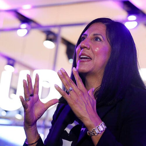
CloudDanielle Royston's Skyvera makes $18M bid for Casa's wireless bizDanielle Royston's Skyvera makes $18M bid for Casa's wireless biz
Skyvera, the company tied to Danielle Royston, made a surprise $18 million bid for Casa Systems' wireless business. But how that bid might impact Verizon – Casa's main wireless customer – is unclear.


Latest News


Popular whitepapers in 5G


May 21 - May 23, 2024
May 21 - May 23, 2024
Join us for an immersive experience where the future of North American telecom industry unfolds in 2024.
LEARN MOREFeatured Videos


Subscribe and receive the latest news from the industry.
Join 62,000+ members. Yes it's completely free.